
ORT82G5-G2-PAC-EV
Vergleichen Sie
ORT82G5-G2-PAC-EV
BOARD BRIEFCASE ORT82G5 SERDES


Vergleichen Sie
Preis verhandelbar
Preisaktualisierung:vor einem Monat
Auf Lager verfügbar:
4439


45
Bedient Kunden in 45 Ländern
1000+
Weltweite Hersteller
$140M
$140M Wachstum in 5 Jahren
50.0M+
50 Millionen ausgelieferte Teile in 5 Jahren

Lattice Semiconductor Corporation
Lattice Semiconductor ist der Marktführer bei programmierbaren Produkten mit geringem Stromverbrauch. Sie lösen Kundenprobleme im gesamten Netzwerk, vom Edge bis zur Cloud, in den wachsenden Kommunikations-, Computer-, Industrie-, Automobil- und Verbrauchermärkten. Ihre Technologie, ihre langjährigen Beziehungen und ihr Engagement für erstklassigen Support ermöglichen es ihren Kunden, ihre Innovationen schnell und einfach umzusetzen und eine intelligente, sichere und vernetzte Welt zu schaffen.
Alle Produkte ansehen von Lattice Semiconductor Corporation


The ORT42G5 and ORT82G5-G2-PAC-EV provide a clockless high-speed interface for interdevice communication on a board or across a backplane. The built-in clock recovery of the ORT42G5 and ORT82G5-G2-PAC-EV allows for higher system performance, easier-to-design clock domains in a multiboard system, and fewer signals on the backplane. Network designers will benefifit from the backplane transceiver as a network termination device. The device supports embedded 8b/10b encoding/decoding and link state machines for 10 G Ethernet, and Fibre Channel.
The ORT82G5-G2-PAC-EV is pinout compatible with a sister device, the ORSO82G5, which implements eight channels of SERDES with SONET scrambling and cell processing. The ORT42G5 is pin compatible with the ORSO42G5,which implements four channels of SERDES with SONET scrambling and cell processing.
Feature
• High-performance programmable logic:
– 0.16 µm 7-level metal technology.
– Internal performance of >250 MHz.
– Over 400K usable system gates.
– Meets multiple I/O interface standards.
– 1.5V operation (30% less power than 1.8V operation) translates to greater performance.
• Traditional I/O selections:
– LVTTL (3.3V) and LVCMOS (2.5V and 1.8V) I/Os.
– Per pin-selectable I/O clamping diodes provide 3.3V PCI compliance.
– Individually programmable drive capability: 24 mA sink/12 mA source, 12 mA sink/6 mA source, or 6 mA
sink/3 mA source.
– Two slew rates supported (fast and slew-limited).
– Fast-capture input latch and input Flip-Flop (FF)/latch for reduced input setup time and zero hold time.
– Fast open-drain drive capability.
– Capability to register 3-state enable signal.
– Off-chip clock drive capability.
– Two-input function generator in output path
• New programmable high-speed I/O:
– Single-ended: GTL, GTL+, PECL, SSTL3/2 (class I and II), HSTL (Class I, III, IV), ZBT, and DDR.
– Double-ended: LVDS, bused-LVDS, and LVPECL. Programmable (on/off) internal parallel termination (100
Ω) is also supported for these I/Os.
• New capability to (de)multiplex I/O signals:
– New DDR on both input and output at rates up to 350 MHz (700 MHz effective rate).
– New 2x and 4x downlink and uplink capability per I/O (i.e., 50 MHz internal to 200 MHz I/O).
• Enhanced twin-block Programmable Function Unit (PFU):
– Eight 16-bit Look-Up Tables (LUTs) per PFU.
– Nine user registers per PFU, one following each LUT, and organized to allow two nibbles to act independently, plus one extra for arithmetic operations.
– New register control in each PFU has two independent programmable clocks, clock enables, local SET/RESET, and data selects.
– New LUT structure allows flflexible combinations of LUT4, LUT5, new LUT6, 4 → 1 MUX, new 8 → 1 MUX, and ripple mode arithmetic functions in the same PFU.
– 32 x 4 RAM per PFU, confifigurable as single- or dual-port. Create large, fast RAM/ROM blocks (128 x 8 in only eight PFUs) using the Supplemental Logic and Interconnect Cell (SLIC) decoders as bank drivers.
– Soft-Wired LUTs (SWL) allow fast cascading of up to three levels of LUT logic in a single PFU through fast internal routing which reduces routing congestion and improves speed.
– Flexible fast access to PFU inputs from routing.
– Fast-carry logic and routing to all four adjacent PFUs for nibble-wide, byte-wide, or longer arithmetic functions, with the option to register the PFU carry-out.


Produkt-Eigenschaften
| TYP | BESCHREIBUNG | Alle auswählen |
|---|---|---|
| Serie | ORCA® Serie 4 | |
| Paket | Schüttgut | |
| Produktstatus | Veraltet | |
| Typ | FPGA | |
| Zur Verwendung mit/verwandten Produkten | ORT82G5 | |
| Inhalt | Platine(n), Kabel(e), Netzteil |
Blog


 Ein tiefer Einblick in den globalen Markt für KeramikkondensatorenErforschen Sie mit uns die aufkommende Nebenhandlung des Umweltbewusstseins auf dem globalen Markt für Keramikkondensatoren.
 Beherrschen der Strommessung mit MikrocontrollernEntschlüsseln Sie die Geheimnisse der präzisen Strommessung mit Mikrocontrollern! Bewältigen Sie Herausforderungen, finden Sie Superhelden-Lösungen und revolutionieren Sie die Genauigkeit mit On-Chip Analog Core Independent Peripherals (CIPs).
 Was ist eine Gleichrichterdiode: Ein Leitfaden für EinsteigerLernen Sie die unbesungenen Helden der Elektronik kennen - Gleichrichterdioden! Erforschen Sie ihre Magie, ihre Anwendungen und nehmen Sie teil an dem Abenteuer hinter den Kulissen der Geräteleistung.
 FPGAs im Wettstreit: XC6SLX16 gegen XC6SLX25Entschlüsseln Sie die Geheimnisse der FPGAs mit unserer Kurzanleitung! XC6SLX16 oder XC6SLX25 - welcher ist der Schlüssel für Ihr nächstes technisches Abenteuer? Klicken Sie jetzt und entdecken Sie die Welt der programmierbaren Möglichkeiten!
 Mehr Sicherheit im Straßenverkehr mit fortschrittlichen Bildsensoren von onsemiLernen Sie den AR0220AT von onsemi kennen, einen nächtlichen Wegbereiter für fortschrittliche Fahrerassistenzsysteme.


Preis verhandelbar
Preisaktualisierung:vor einem Monat
Auf Lager verfügbar:
4439
Lattice Semiconductor Corporation
Lattice Semiconductor ist der Marktführer bei programmierbaren Produkten mit geringem Stromverbrauch. Sie lösen Kundenprobleme im gesamten Netzwerk, vom Edge bis zur Cloud, in den wachsenden Kommunikations-, Computer-, Industrie-, Automobil- und Verbrauchermärkten. Ihre Technologie, ihre langjährigen Beziehungen und ihr Engagement für erstklassigen Support ermöglichen es ihren Kunden, ihre Innovationen schnell und einfach umzusetzen und eine intelligente, sichere und vernetzte Welt zu schaffen.
Alle Produkte ansehen von Lattice Semiconductor CorporationBlog
- Ein tiefer Einblick in den globalen Markt für KeramikkondensatorenErforschen Sie mit uns die aufkommende Nebenhandlung des Umweltbewusstseins auf dem globalen Markt für Keramikkondensatoren.
- Beherrschen der Strommessung mit MikrocontrollernEntschlüsseln Sie die Geheimnisse der präzisen Strommessung mit Mikrocontrollern! Bewältigen Sie Herausforderungen, finden Sie Superhelden-Lösungen und revolutionieren Sie die Genauigkeit mit On-Chip Analog Core Independent Peripherals (CIPs).
- Was ist eine Gleichrichterdiode: Ein Leitfaden für EinsteigerLernen Sie die unbesungenen Helden der Elektronik kennen - Gleichrichterdioden! Erforschen Sie ihre Magie, ihre Anwendungen und nehmen Sie teil an dem Abenteuer hinter den Kulissen der Geräteleistung.
- FPGAs im Wettstreit: XC6SLX16 gegen XC6SLX25Entschlüsseln Sie die Geheimnisse der FPGAs mit unserer Kurzanleitung! XC6SLX16 oder XC6SLX25 - welcher ist der Schlüssel für Ihr nächstes technisches Abenteuer? Klicken Sie jetzt und entdecken Sie die Welt der programmierbaren Möglichkeiten!
- Mehr Sicherheit im Straßenverkehr mit fortschrittlichen Bildsensoren von onsemiLernen Sie den AR0220AT von onsemi kennen, einen nächtlichen Wegbereiter für fortschrittliche Fahrerassistenzsysteme.
Beliebte Hersteller
View all manufactures Mehr


Beliebte Teile Nummer
Weitere elektronische Bauteile Mehr
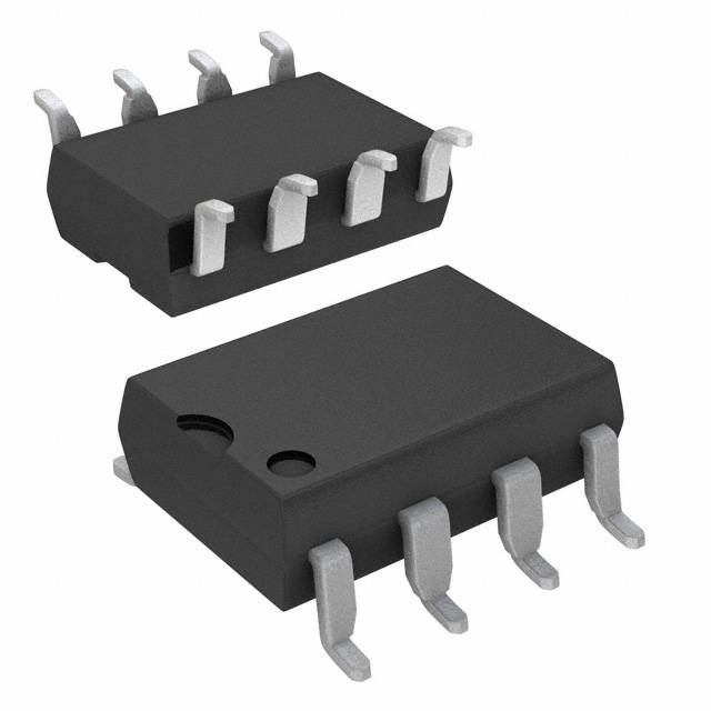
VO2601
OPTOISO 5.3KV OPEN DRAIN 8DIP
VOD3120AG
OPTOISO IGBT MOSFET DRIVER 2.5A
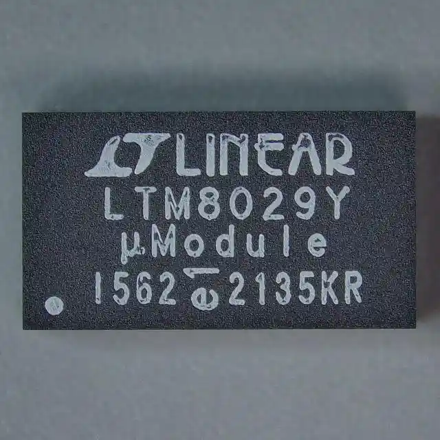
LTM8029EY#PBF
DC DC CONVERTER 1.2-18V
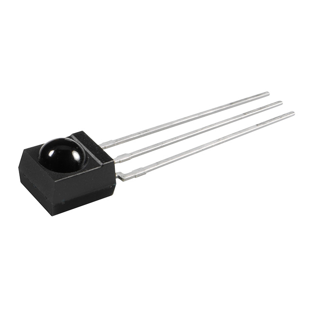
TSOP18440
SENSOR REMOTE REC 40.0KHZ 24M
VOW3120-X017T
OPTOISO 5.3KV 1CH GATE DRVR 8SMD
VO3120-X019T
OPTOISO 5.3KV 1CH GATE DRVR 8SMD
VOW137-X001
WIDEBODY, HIGH ISOLATION, HIGH S
TSOP13540
SENSOR REMOTE REC 40.0KHZ 30M
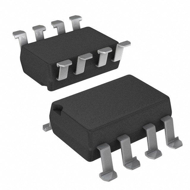
LTC2053HMS8#PBF
IC OPAMP ZERO-DRIFT 1 CIRC 8MSOP
VO2601-X007T
OPTOISO 5.3KV OPEN DRAIN 8SMD